Table of Contents
1. Basics of Laser Diode
1.1. About Laser Diode
A laser diode is a general term for amplifiers and oscillators of light waves, which uses stimulated emission of the grid due to the optical transition of electrons in semiconductors. The idea of laser diodes had already appeared in 1957, and pioneering studies had begun not long after the demonstration of the oscillation of He-Ne laser and ruby laser in 1960. Cold pulse oscillation of a GaAs laser (the first laser diode) was observed in 1962, and in 1970 room temperature continuous wave operation was achieved. After this laser diode technology has developed remarkably starting the light electronics era. In present time it is used in many fields such as optical recording and optical communications.
1.2. Optical Amplification Gain and Stimulated Emission in the Laser Diode
This section will state the basic characteristics and basic theory of carrier injected stimulated emission in semiconductors and optical amplification gain. The former is the most important principle that makes laser diode possible. The latter is the most important parameter when performing laser characterization.
1.2.1. Band Structure of a Direct Transition Type Semiconductor
Laser diodes are realized by utilizing the interband optical transitions of carriers in semiconductors with a direct transition type band gap. As it is well known in solid-state electronic theory, the wave function of electron wave vector k of an ideal semiconductor crystal can be said as following, when Bloch function uk(r) is normalized by unit volume.
![]()
Electronic such as this forms a band structure and forms a continuous energy levels. Figure 1.2.1 shows a schematic diagram of the band structure of a typical material for laser diodes, GaAs. Ⅲ-Ⅴ compound semiconductors such as GaAs is a zinc-blende-type crystal structure. The valence band and the conduction band is caused formed by a sp3 hybrid orbital that implements a covalent bond. Therefor the conduction band consists of a single conduction band, the valence band is composed of heavy hole band, light hole band, and the split-off band. Because the center of k-space (Γ point) is at the top of the valence band, the k that determines the band gap is equal at the upper edge of the valence band and at the lower edge of the conduction band. This is called the direct-transition-type band gap. The law of conservation of momentum of the electrons are met, upon transitioning between with absorbance and emission of photons whose energy is close to the band gap energy Eg. For this reason, transition probability is high, and is used for laser oscillating. Most Ⅲ-Ⅴ compound semiconductors (such as GaAs, AlGaAs, InP, and InGaAsP) and Ⅱ-Ⅵ compound semiconductors have a direct-transition-type band gap. Ⅳ group semiconductor Si, Ge, and Ⅲ-Ⅴ group AlAs has an indirect-transition-type band gap where the k is not equal at the upper edge of the valence band and at the lower edge of the conduction band. Semiconductors that are indirect-transition-type is not suitable for laser diode, because transition probability is low due to the optical transition interacting with the phonons.
Electronic energy near band edge of the conduction band and the valence band can be derived by the following equations when the wave vector of the electron is set as k.
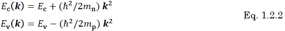
Band structure represented by this equation becomes a parabolic function type. Ec and Ev represents the energy of the lower end of the conduction band and the upper end of the valence band, respectively. Ec-Ev represents band gap energy Eg. mn and mp represents effective mass of electrons in the conduction band and effective mass of holes in the valence band, respectively. Density of states of electrons in the conduction band and the valence band is represented by the following equations.
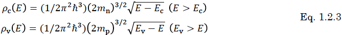
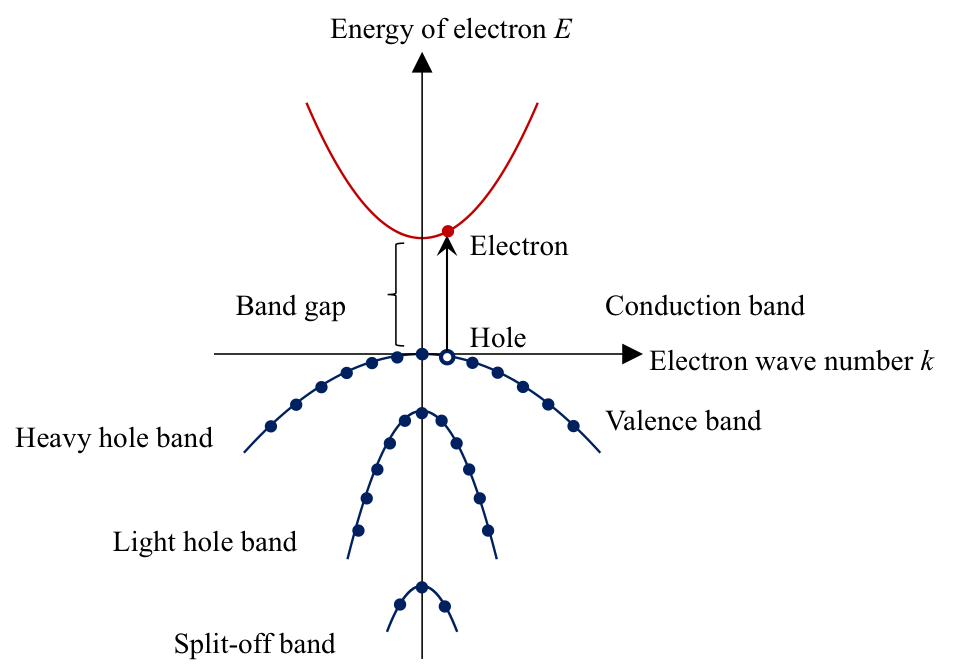
Fig. 1.2.1. The band structure of GaAs around Γ point.
1.2.2. Conditions for Stimulated Emission
Considering the condition for the stimulated emission to be achieved in an optical transitions of electrons in semiconductors when viewing it as a simple inter-band transition energy that satisfies the conservation law. Figure 1.2.2 shows the model.
Generally, when a system is at thermal equilibrium, the possibility f of the level which the energy is E being occupied by electrons is described as the following Fermi-Dirac function.
![]()
Here F is Fermi level, kB is Boltzmann’s constant and T is absolute temperature of the system.
Although a net stimulated emission cannot be obtained when in the thermal equilibrium state, however it is possible to achieve a population inversion by injecting minority carriers that have higher energy than the majority carriers, with such methods as passing a current through the semiconductor’s PN junction. In a semiconductor that has been excited by minority carrier injection, thermal equilibrium is not achieved between the valence band and the conduction band. When thinking of the pseudo-thermal quasi-equilibrium state approximation where within each band is regarded as an approximate equilibrium state, the probability of the level of E1 of the valence band and level of E2 of conduction band being occupied by electrons is given by the following equation.
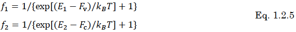
The Fv and, Fc here are valence band and quasi-Fermi level of the conduction band, respectively. The state represented by the above equations is called a pseudo-thermal quasi-equilibrium state. By applying a forward voltage V to the semiconductor PN junction, the energy difference of eV is given to the Fermi level of the N region and P region. As a result, careers are injected from the N region and the P region into the active region and then the difference Fc-Fv of quasi-Fermi level become to be equal to eV.
In order to obtain a light amplifying effect by stimulated emission, more net stimulated emission than absorption is required, also must satisfy the following equation.
![]()
This indicates that population inversion is required.From Eq. 1.2.5 and 1.2.6, it can be rewritten as
![]()
In other words, it is understood that in order to obtain the optical amplification effect, it is necessary to satisfy eV>E2-E1 (=ℏω).
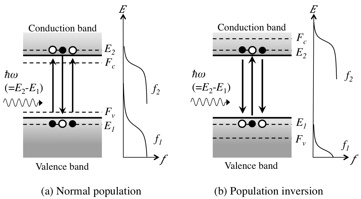
Fig. 1.2.2. Absorption and emission of photons by electron transition in semiconductors that are carrier injected.
1.2.3. Absorption, Gain coefficient, Absorption and Emission of Photons
After analyzing the absorption and emission release of photons taking in to consideration the fact that, electrons in the semiconductor band structure is represented by a set of many states with a continuous energy, leading a basic formula for calculating the gain of the optical amplification caused by laser action. Considering the case of the light waves of a single mode of each frequency ω incidents in to the semiconductor, the refractive index of the semiconductor is nr, group index is ng, light wave mode is normalized by the volume V and number of photons is n.
Probability of stimulated emission and absorption probability of electrons in the initial state per couple in the final state per couple per and per unit time are represented as the following equation.
![]()
+ of – represents the absorption and the – represents the emission, respectively.
To represent the whole optical transition, it is needed to integrate electronic state of all combinations.
Absorption coefficient α that represents the light absorption is defined by relative decrease in intensity per unit distance as α=(-dI/dξ)/I where I is the light intensity and ξ is coordinate axes taken in the light wave traveling direction.
This is the product of net number of absorption transition photon absorbed per unit volume and per unit time (= number of photon absorbed transition – the number of photon stimulated emission transition), and single photon energy ℏω. On the other hand, light intensity I is given by the light energy (not including the zero-point energy) that traverses the unit cross-sectional area in unit time, therefore the light intensity can be expressed as follows using number of photons n and group velocity of the light wave vg.
![]()
From this, α is ℏω/I=(V/n)(ng/c) times larger twice than net number of transition photons absorbed transition number per unit volume and per unit time ℏω/I=(V/n)(ng/c). In addition, the gain coefficient g representing to the light amplification is defined by g=(dI/dξ)/I(=-α). In the calculation of α corresponds to the net absorption (= absorption transition – stimulated emission transition) and in the calculation of g corresponds to the net stimulated emission (= stimulated emission transition – absorption transition).
1.3. Analysis Model of a Direct Transition Semiconductor
Assuming a semiconductor with a direct-transition-type band gap is a pure perfect crystal, consider the optical transitions of electrons in the near band edge. In this case, while transition in which wave vector k is conserved is only considered, to be exact upon transition it is necessary to consider the law of conservation of momentum of the whole electron and photon in the system. However, it can be ignored for the wave number of the photon that is very small compared to the wave number of electrons.
Assuming the matrix elements of the momentum of the wave function of the electron is M and the average of the mean square is |M|2, absorption coefficient α and the gain coefficient g is given by the following equation.
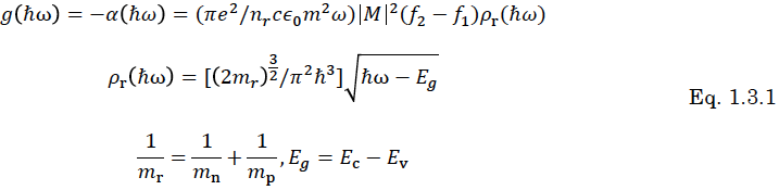
ρr, mr, and Eg represents the equivalent density of states, respectively. Because g is proportional to the product of ρr and occupation probability differential f2-f1, the approximate ω dependence of g depends on ρr and f2-f1.
The spontaneous photon emission from the semiconductor per unit volume and per unit time can be expressed by the following equation.

The power of the spontaneous emission light can be gained by the product of rspt dω and photon energy ℏω.
Mathematical model showing a light absorption and emission of a direct-transition-type semiconductor described above, is enough for qualitatively understanding, but it is necessary to be careful when considering the quantitative. This is because, although semiconductors used in laser diode are direct-transition-types, when with impurities doped, transition which does not satisfy the wave vector conservation law occurs. It is especially inappropriate when having a detailed discussion of optical transition near the band edge quantitatively.
1.4. Model Representing the Actual Energy State of the Semiconductor (GHLBT-SME model)
Light absorption and emission, including the transition that does not satisfy the wave vector conservation law, can be analyzed by integrating transition probabilities by energy.
When net stimulated emission coefficient per unit volume and per unit time is integrated by energy, the gain coefficient g is given by the following equation.

Also, with the spontaneous emission, photon emission rate per unit time and per unit volume in the frequency range between ω and ω+dω can be represented by the following equation.

In other words, the spontaneous emission light power in the narrow frequency range from a semiconductor per unit volume can be given from rspt(ℏω)dω and ℏω.
Models that the band structure has a clear edge, and the state density is assumed to be a parabolic function can be applied as a good approximation to a pure semiconductor. However, it cannot be easily handled as this, because normal semiconductors used for laser diodes doped with impurities. Impurity that has small effective mass doped in semiconductors can be easily ionized. When doping density is larger than a certain extent, carriers supplied from impurities contribute to conduction at all times. For this reason, to regard the impurity level as localized level is not adequate. Because impurity ions are mixed randomly into the crystal, it is necessary to consider that the periodic potential of the lattice is disturbed causing a tail in the density of states of the conduction band and the valence band. Such a model is called the band tail model. Band tail was first modeled by Kane. However this model ignored the kinetic energy of the carrier’s, density of states of the band tail was excessive.
After this the model was properly altered by Halperin and Lax, after which Stern compromised the two models. A convenient method that can express the density of states of the entire area around the band edge by a simple function has been proposed. This model is under the name of Gaussian Halperin-Lax bandtail model (GHLBT).
In order to calculate momentum matrix element |M|2, electron wave function of the valence band and the conduction band is needed. In an ideal semiconductor crystal wave function of the electron can be described as in Eq. 1.2.1. However, in a semiconductor which contain impurities it is necessary to consider electrons near the band edge (k~0) are localized by the effects of the impurities. Electron wave functions of this kind are able to be represented using an envelope function representing the localization. From this it is possible to determine the momentum matrix elements of the semiconductor crystal containing impurities. At this time, also requires consideration of the influence of a decrease in the effective energy by localization. Matrix elements which consider this influence is under the name Stern’s matrix element (SME).
Spontaneous emission spectrum and the light absorption calculated using the GHLBT-SME model are agreed well with experimental results, thus confirming the validity this model. By using this model, it is possible to quantitatively evaluate the gain of a semiconductor that is doped with impurities. Gain spectrum by GHLBT-SME model shows the same tendency as the result of the direct-transition model. However, it has a smooth shape in the vicinity of the band gap energy due to the contribution of the band tail.
High carrier density required to achieve a gain is achieved by current injection. With the injection level below the laser oscillation threshold, the carrier is mainly consumed by recombination due to photon spontaneous emission. However, since the number of spontaneous emission per unit time is given by a function of the carrier density N, N is associated with the injection current density J. It is possible to work out from analyzing the gain spectrum with the injected current density, the carrier density dependence and the injection current dependence of the maximum gain. Both of these are represented by the following linear functions.
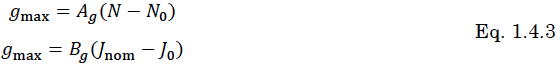
N0,J0 is the transparency current density and transparency carrier density respectively, and Ag,Bg is the differential gain. In an actual laser, the carrier is consumed not only by the spontaneous and stimulated emission recombination, but also by non-radioactive recombination by the Auger process and defects in the crystal structure. Because of this, the value of effective injection current is obtained by multiplying it with the internal quantum efficiency.
One simple and accurate method of gain analysis is density matrix analysis.
In this analysis, the effect of non-direct transition is treated as inter-band relaxation, also the gain spectrum can be given by the following equation.
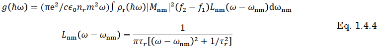
This result is a convolution of the direct-transition model equation (11) and Lnm (ω-ωnm).
Here it is ℏωnm=En-Em where En,Em, and τr are conduction band electron energy, valence band electron energy, and relaxation time, respectively. Lnm (ω-ωnm) is under the name of line shape function, when τr→∞ it becomes Lnm (ω-ωnm)→δ(ω-ωnm).Gain characteristics of a number of materials have been found with this method. It is also possible to analyze the effects such as gain saturation and spectral hole burning caused by deviation from the quasi-thermal equilibrium state of the carrier energy distribution.
1.5. The Stimulated Emission in a Semiconductor Quantum Well Structure
1.5.1 Electronic States and the Quantum Well Structure
A double hetero (DH) structure composed of a thin semiconductor layer of a few nm is called a quantum well (QW). The film thickness is close to the electron wavelength thus the electrons are confined in the film as a wave. For this reason, different physical properties from the thick bulk double hetero structure appear, making it able to be used for performance improvement and enhancements. In recent years QWs are widely used in laser diodes.
Figure 3 shows the arrangement of the valence band and the conduction band of the QW.
Conduction band electrons are confined in the potential well allowing them only to move in the direction along the QW plane. The envelope wave function of the conduction band electrons in the direction perpendicular to the plane has a discrete distribution as shown in Fig 1.5.1. Momentum dependence of energy of the n-th electron of distribution χn (z) in the plane is represented by the parabola which is concave up with a vertex that is eigenvalues εn above than the lower edge of the conduction band. Also the conduction band has multiple sub-band structure. Also the conduction band takes multiple sub-band structure. The n-th sub band’s density of states is 0 at E<εn, and is constant value at E>εn. Therefore, electronic density of states of the entire conduction band ρ2D (E) becomes a staircase shape as shown in Fig. 1.5.2. There is a difference between the ρ2D (E) of electronic density of states of the entire conduction band and ρ2D (E) of bulk density of states: electronic density of states rises sharply at εn and bulk density of states is given by the parabolic function. Sub-band is also formed in the valence band electrons. While valence band consisting of light hole band and heavy hole band, forms a complex sub-band structure in the QW, it is the same in the way that it has a step-shape property.
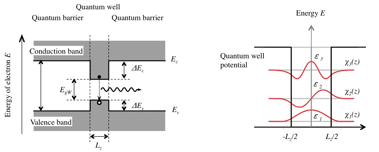
Fig. 1.5.1. The confinement of the electron wave in the quantum well
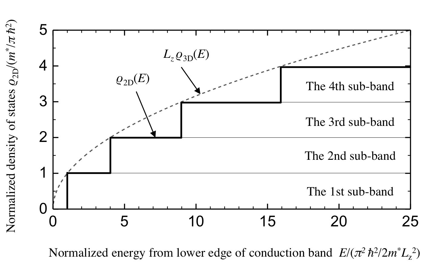
Fig. 1.5.2. Two-dimensional density of states of the quantum well and the three-dimensional density of states of the bulk semiconductor.
1.5.2. Gain characteristics of a quantum well structure
Gain spectrum of the quantum well can be expressed as a direct transition model Eq. 1.3.1 or a Eq. 1.4.4 that takes into account the relaxation effect. However, there are important differences compared with the bulk. Matrix element |M|2 is a small value thus only transitions that satisfies quantum number conservation law occurs, except when sub-band number n of electrons and holes are equal. Furthermore, |M|2 has polarization dependence: the values of light polarized parallel to the QW plane (TE wave) is greater than the value of the vertical polarization (TM wave). For density of states it is necessary to use ρ2Dr(ℏω) which is two-dimensional, also ρ2Dr(ℏω) can be gained by step function in response to the stepwise ρ2D (E).
Figure 5 shows the gain spectrum of the quantum well obtained by the direct transition model. Gain is dominated by the contribution of only the first sub-band when the injection level is not high, and can be obtained in the form of a product of f2-f1(ℏω) that rises in a step shape at E(g,1) which is a point that is shifted ε(1,e)+ε(1,h) from Eg. Therefor gain shows a narrow peak that rises sharply at E(g,1).
QW laser has the following features compared to the bulk DH lasers that have an active layer with same composition:
① It oscillates at a shorter wavelength since QW laser has eigenvalue ε(1,e)+ε(1,h).
② Shift of the gain peak wavelength due to the band filling is small.
③ Gain increases corresponding to carrier density increase after transparency, however after which shows saturation trend.
④ Gain is less affected by temperature changes.
⑤ TE wave gain is larger than TM wave gain.
It is possible to use straight-line approximation as in Eq. 1.4.3 for carrier density dependence of maximum gain, however because there is a tendency as ③, logarithmic function approximation represented by the following can be applied with a higher precision.

DH structure consists of lattice-matched mixed crystal combinations. However, due to the QW thinness it is possible to construct QW with a combination that has slightly lattice mismatched.
QW at this time becomes a strained quantum well that has compressive strain or extension strain.
Because the strain changes the band structure, it can be used for bringing out useful property to improve laser performance with proper designing. An important effect is that the effective mass of the holes is reduced and the curvature of the valence band is increased. Because of this balance between the conduction band and the valence band is improved and carrier density required to achieve population inversion is reduced. Therefore, as transparency current density is reduced differential gain also increases thus making it possible to make it low threshold or high output.
Furthermore, in a strain quantum well the degeneracy of the upper end of the light hole band and heavy hole band is resolved, leading to be making electron-heavy hole transition be main transition with a compressive stain QW and electron-light hole transition be main transition with a extension strain QW. Since the former contributes to the amplification of the TE wave and the later contributes to the amplification of the TM wave, by applying the proper strain it is possible to control the polarization dependency of amplification characteristic and oscillation characteristics.
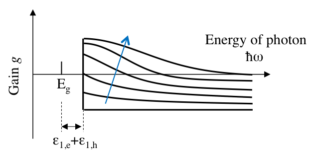
Fig. 1.5.3. Variation of the gain spectrum obtained when increasing the carrier injection into the semiconductor quantum wells.
1.6. Materials and Structure of Laser Diode
A basic laser diode is made by constructing a double hetero (DH) structure to inject carriers into the active layer and confining it at a high density, this is constructed by joining the active layer used for light amplification and a cladding layer that has a wider band-gap than the active layer.
The oscillation wavelength λ of the laser diode is determined by the band gap energy Eg of the active layer material. Because of this usually the required oscillation wavelength is gained by using compound semiconductor mixed crystals. Fig 1.6.1 shows the important oscillation wavelength region and laser diode material. A good example is AlxGa(1-x) As a mixed crystal of GaAs and AlAs, and it is possible to set the oscillation wave length in the range of 0.7~0.9 μm.
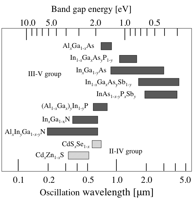
Fig.1.6.1. Important laser diode material
and oscillation wavelength region.
Figure 1.6.2 shows the band structure distribution of DH lasers. With a bulk’s DH laser an active layer with a thickness of about 0.1 μm is used. The active layer is sandwiched by the p-type cladding layer and the n-type cladding layer. In a thermal equilibrium state the electrons and holes exist separately in the n-type region and the p-type region. If a forward bias voltage is added to the junction, the potential of the n-type region is up injecting a small number of carriers. Due to this conditions for stimulated emission is met performing light amplification. With Ⅲ-Ⅴ compound semiconductors refractive index can be made smaller by changing the composition ratio making Eg larger. As a result light wave is trapped in the active layer due to total reflection working as a optical waveguide. By confinement of the light wave and carrier, it is possible to achieve high efficiency laser oscillation. Different structures are used for carrier confining, from single quantum wells to multiple quantum wells (Fig. 1.6.3).
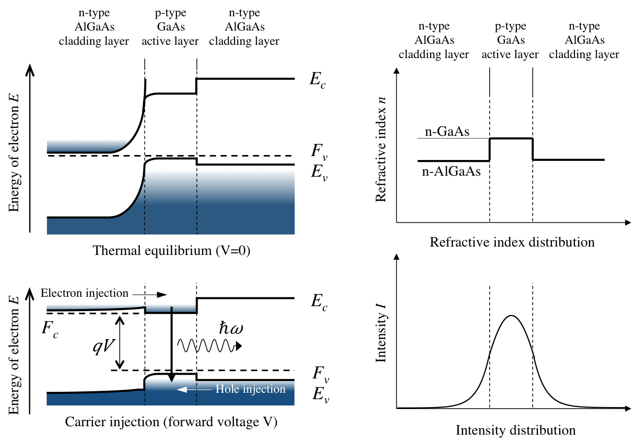
Fig. 1.6.2. The confinement of the light wave and carriers
in the DH structure laser diode.
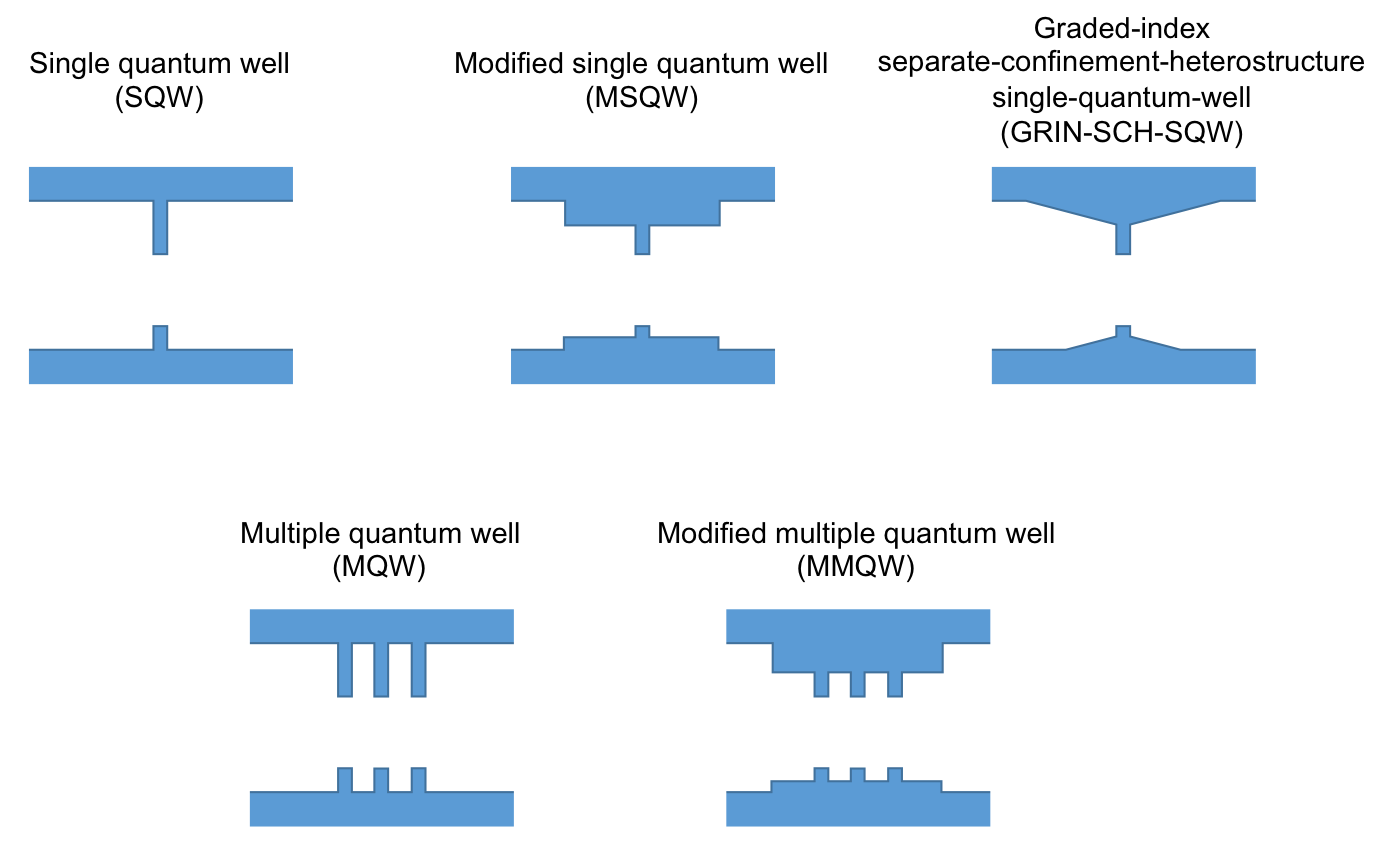
Fig. 1.6.3. Schematic diagram of a stripe laser diode.
Because semiconductor has a high refractive index, about reflectance of 35% is obtained with a simple cleavage facet. Because of this it is possible to form a Fabry-Perot type optical resonator without using a mirror. The mainstream of high coherence and low ~ middle output strength lasers is stripe type lasers, which has limit to the carrier injection and light wave propagation to a narrow channel-shaped area. Figure 1.6.4 shows the schematic diagram. It consists of a channel optical waveguide that has a thin core region of high refractive index and a current confinement structure. Light distribution in the waveguide cross section is called the transverse mode, and the waveguide is designed to guide only the fundamental mode.
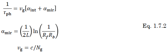
Light wave is circulated while being amplified in the waveguide structure. Until now this tutrial has stated about the gain coefficient assumed the light wave propagates only though the active layer, however in reality it is necessary to take in to account cavity loss and leakage of the guided mode. When if Γ is the ratio of active region power and total intracavity power (Confinement factor), the gain is reduced by Γ times. Also if considering internal loss αint the effective gain for the waveguide mode becomes Γg-αint.
Laser oscillating condition can be expressed by the following equation, where Rf,Rb is the reflectivity of the mirror front and back of the resonator, L is the resonator interval, Ne is the effective refractive index of the waveguide mode for each frequency ω, and m is any integer value.
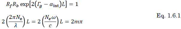
The first equation represents the amplitude conditions and the second expression represents the phase condition. Each resonation frequency that meets this is called longitudinal mode. The spacing of adjacent longitudinal mode can be obtained by ω=2π(c/2NgL) (Effective refractive index: Ng=Ne+ω∂Ne/∂ω). When the effective gain of a longitudinal mode reaches a value that satisfies the first equation oscillation of this longitudinal mode can be obtained.
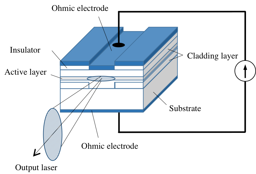
Fig. 1.6.4. Various quantum well structure.
1.7. Basic characteristic of Laser Diode
1.7.1. Rate equation
Most common and effective method to analyze the characteristics of laser diodes is rate equation analysis.
Time dependent variation of carrier density N and photon density S inside the active layer are given by the equation below.
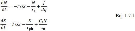
The first term, the second term and the third term in the first equation each represent simulated emission recombination, spontaneous emission recombination and current injection. The first term, the second term and the third term in the second equation each represent stimulated emission, decay of phonons and spontaneous emission. τs, J , d , and q each represent carrier lifetime, injected current density, thickness of the active layer and elementary charge. τph is photon lifetime and in FP laser, this is given using the equation below by using inside loss αint,reflection ratio of the front and back facet mirror Rf,Rb and resonator length L.
vg is group delay and Cs is the spontaneous emission coupling coefficient which represents the contribution to oscillation mode amongst all spontaneous emission N/τs. In normal cases it is Cs<<1.
G is time dependent gain factor and the relationship to vgg is G=vgg.
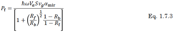
Available output-power Pf is described as the following equation. Also, this is proportional to the photon density S.
The case above the equation was used for a single mode-oscillation, however by defining photon density Sm of multi-mode m it is possible for the equation to be expanded for multi mode use.
1.7.2. Stationary oscillation characteristic
Through solving the rate equation in stationary state, injection current J dependency of carrier density N and photon density S can be obtained. In a case where the injection current is small, coherent radiation can not be obtained, however when N reaches threshold carrier density Nth=N0+1/ΓAτph, oscillation condition ΓG=1/τph is satisfied, obtaining coherent radiation. In a Bulk DH structure, gain G has the same value as TE wave and TM wave. However the TE wave facet mirror reflection ratio R has a larger value to the TE wave, thus TE wave has a lower threshold gain value. Therefore, FP laser of bulk DH structure oscillates TE waves.
Increase J in the region above the threshold doesn’t lead to N increasing to maintain oscillation condition. However, because the carrier injected in the region over the threshold is converted into phonon due to stimulated emission, S and out-power P becomes larger in approximately proportionate to J-Jth. In this way, S -J characteristic shows a polygonal line graph that has a kink at the threshold. In a case where spontaneous emission combining Cs is large, the kink has a curved characteristic. Graph slope between light power and current over threshold is called slope efficiency and graph slope between output photon number and injected electron number is called external differential quantum efficiency.
In a case where the cleavage end face is used as mirror in a FP laser, output light is divided into the front part and the back part. Therefore in many cases, the back facet is coated with high reflection coating to obtain reflectance close to Rb=1 leading to the increase of the front output power Pf. Enhancing reflection ratio Rf,Rb can cause the threshold decrease however the slope efficiency also becomes lower. For this reason, to obtain high output power both Rb enhancement and Rf optimization are mandatory.
A normal FP laser diode’s gain range is several times larger than the longitudinal mode’s space and an injection value slightly higher than the threshold douse lead to multimode oscillation. However, as the injection value increases, photon density at center mode increases in proportion to current increment, while the photon density increase of other modes saturate, thus the oscillation comes closer to a single mode oscillation. This tendency depends on spontaneous emission reunion coefficient Cs, the larger the Cs is the wider the range of multi-mode oscillation, and if Cs is a small value it reaches pseudo-single-mode oscillation quickly.
1.7.3. Modulation characteristic
Laser diode can modulate output power by superimposing a signal into the injection current. Since this direct intensity modulation is convenient, highly effective and enables high-speed modulation it is an important characteristic which makes way for many various applications.
Small signal modulation can be analyzed by the following method:
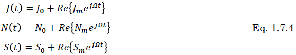
(a) Dividing the drive current, the carrier density and the photon density into bias element which represents the operating point and modulation component that varies sinusoidally in each frequency Ω, as shown in Eq. 1.7.4
(b) Solving the equation related to small signal amplitude Nm,Sm obtained by substituting Eq. 1.7.4 in to rate equation.
Transfer function representing frequency characteristics of intensity modulation is represented as Eq. 1.7.5.
Here, ΩRand ΓR each represent relaxation oscillation frequency and damping ratio of relaxation oscillation. Frequency characteristic is flat in the low-frequency range, but it has the peek at the vicinity of ΩR and it decreases steeply at a higher frequency than ΩR. Also it develops a phase lag as modulating frequency approaches nearer to ΩR. Because the actual maximum frequency is limited by ΩR, sufficient bias current needs to be supplied for high-speed modulation. In the case of a normal laser diode the maximum of a few GHz at high injection level. However, by using methods such as quantum wells it is possible to achieve a modulation bandwidth of a few dozen GHz. From rate-equation analysis of small signal step response, it can be sed that carrier density and output power become asymptote to steady state after making damped oscillation for 1/ΓR at frequency ΩR when injected current is changed stepwise. This vibration is called relaxation oscillation and it is caused due to the following reasons: (a) Carrier density changing later than the current injection changing. (b) Photon density not being able to change faster than the photon lifetime due to the light wave circulating in the resonator. When direct intensity modulation as above is operated, refractive index also changes with time as carrier density changes with time. Consequently output light phase is modulated and frequency modulation(FM)is also made. Time-average spectrum of output light moves from narrow single peak into diphasic distribution and distribution range increases with increasing driving current modulation amplitude Jm. Optical frequency modulation by driving current modulation of this kind is called frequency chirping, and limits transmission band and transmission distance in optical communication applications.
In order to understand large amplitude modulation characteristic, multimode rate equation needs to be solved numerically. By injecting a step current into a FP laser, the increase in carrier density begins simultaneous to the injection, and photon density increases steeply soon after the carrier density reaches the threshold and then oscillation is obtained. Oscillation delay can be avoided by giving the bias current close to the threshold. Just after the oscillation, large-amplitude relaxation oscillation occurs and quasi-single mode stationary oscillation is obtained after the decrease in a few nanoseconds.
Note that at this time, large-amplitude-relaxation oscillation occurs not only with the center-mode but also the side-mode. This means that even quasi-single mode oscillation laser becomes multi-mode oscillator by high-speed large amplitude modulation over 100 MHz order.
1.7.4. Noise characteristic
Noise with stationary oscillation can be analyzed by an equation group which has added Langevin noise source (which represents quantum fluctuation) to light wave phase rate equation, carrier density, and photon density.
Intensity noise is represented by power spectrum Sp (Ω) which is the fluctuation δP(t) of the output power P, or relative intensity noise RIN(Ω)=Sp(Ω)/P2 which is made by normalizing power spectrum Sp(Ω). In general RIN is close to flat in the low-frequency area and has the peak close to resonance of excess noise near the relaxation oscillation frequency ΩR and comes close to standard quantum limit 1/P when it is over ΩR. Also, the increase P leads to the decrease of RIN, except when at relaxation oscillation peak. Frequency noise is represented by power spectrum Sω (Ω) obtained from instantaneous frequency fluctuation δω(t) of the output light. Frequency noise is dominated by the refractive index fluctuation due to carrier density fluctuation.
Various kinds of FP laser oscillates with a quasi-single mode. However depending on the condition it oscillates with a mode-hopping phenomenon where oscillation wavelength changes alternatively. This creates a large intensity noise in the frequency region under a few dozen MHz. Even if mode-hopping phenomenon dosnnot occur because FP lasers do not oscillate in a complete single-mode, output light includes both main-mode component and side-mode component. Result of single-mode analysis can be applied to the entire output light. However, if each mode’s component needs to be analyzed separately, noise is generated in low-frequency range due to the random photon distribution inside each of the modes. In order to decrease the noise to a negligible level a side-mode suppression ratio Rsms of 40~50 dB is needed. Such high Rsms can not be obtained by FP laser, however can be achieved by a DFB or DBR laser.
Significant noise generates and the operation becomes unstable upon returning output light by optical component. Therefore, in an application requiring low noise level it is necessary to operate the laser at the low noise region, and to make stable multi-mode oscillation by high-frequency superposed operation or by removal of returning laser by inserting an optical isolator.
1.7.5. Spectrum line width
Output light spectrum linewidth of gas lasers are represented by Schawlow–Townes equation. However, in the case of laser diodes density fluctuation of high-density carrier in active region induces refractive-index fluctuation. Because the fluctuation effects the spectrum it cannot be described with the same equation.
According to a rate-equation analysis which considers fluctuation, optical wave power spectrum is approximately represented by Lorentz function and the spectrum linewidth is given by δω=(CsN/2τsS)[1+αc2]. The first factor (CsN/2τsS) is amended Schawlow–Townes linewidth which means that linewidth comes from fluctuation of spontaneous emission and it becomes narrower with increasing output power. α_c in the second factor called linewidth enhancement factor is the constant number defined by αc=Re{χact}/Im{χact} in relation to carrier-induced complex polarizability χact. It shows the spontaneous emission fluctuation magnified by αc2 times by refractive-index fluctuation. Most laser diode’s linewidth at rated output power is a few dozen of MHz order. However sub-MHz linewidth is achieved by resonator structure design.
1.8. Difference between LED and LD
Both Light Emitting Diode (LED) and Laser Diode (LD) emit light by a current, and have the same combination of semiconductors, if the wavelengths are the same. However they have many differences. Mainly the presence of a resonator structure which LED does not have.
Also LED does not have a stimulated emission which a LD has. Meaning the emitted light from LED is not coherent.
| Item | LED | LD |
|---|---|---|
| Spectrum width | 50 nm | 1〜3 nm |
| Directivity | Have | High |
| Polarization | Non | Linear polarization |
| Modulation rate | 500 MHz | 50 GHz |
1.9. Laser Diode and Semiconductor Optical Amplifier
By performing anti-reflection treatment on the end face of the laser, it is possible to eliminate a cavity structure. Semiconductors with no resonator structure, becomes a light amplifier polarization independence, in a single pass. That is to say, by inputting the laser in to the semiconductor, amplification by stimulated emission is possible. Such device are called Semiconductor Optical Amplifier (SOA).
Antireflection treatment
There are two methods: Formation of the anti-reflection film in the cleavage plane, and to cut diagonally across the surface of the optical waveguide in the active layer is in contact with air. Anti-reflective coating is formed by depositing multiple layers of dielectric having different refractive index.
Performance required for SOA
Important parameter of the SOA are, Small Signal Gain, Saturation Power, and Noise Figure. Parameter of commercially available ones are: Small signal gain of 20 ~ 30 dB, Saturation power of about 10 mW, and Noise of about 5 ~ 8 dB. However it varies depending on the wavelength. The manufacturers of SOA are, Innolume, Inphenix, Superlum, and Thorlabs.
1.10. Higher output power of the laser Diodes
By using a built-in multiple emitters called bar (minibar) in a single module and combining in a single fiber, it is possible to obtain the high power laser diodes for pumping. The following methods can be considered as a combining method.
1. Phase coupling
2. Polarization multiplexing (The use of high polarization extinction ratio in laser diodes)
3. Wavelength multiplexing (The use of broad gain bandwidth in laser diodes)
1.11. Cooling Method of a Laser diode
Thermal management is important in the laser diode.
As a countermeasure, the following four are often used. Cooling capacity increases in the following order.
1. Aluminum heat sink
2. Aluminum heat sink + Cooling fins
3. Aluminum heat sink + Peltier device
4. Aluminum heat sink + Water-Cooled Chiller
Aluminum heat sink
Aluminum heat sink are used for fiber module with 2-pins or TO-Can package with 3-pins.
Cooling fan dissipates heat by applying air to the Aluminum heat sink.
Peltier device
Peltier device takes heat from the heat sink that is in contact with the semiconductor. It needs a pin to send a current to the Peltier device.
Fig. 1.11.1. Inside of the built-in Peltier package
Chiller
A chiller is a machine that removes heat from a liquid via a vapor-compression or absorption refrigeration cycle. This liquid can then be circulated through a heat exchanger to cool air or equipment as required. As a necessary byproduct, refrigeration creates waste heat that must be exhausted to ambient or, for greater efficiency, recovered for heating purposes.
1.12. Method to prevent Laser Diode from being damaged
Static electricity is the natural enemy of lasers diodes. Static electricity accumulated in the human body is about one hundred to several thousand V, but the laser diodes are driven in two to three V. Therefor touching the laser diodes with a charged body, can destroy the laser diode device. To prevent this, When handling a laser diodes, You must put on a hats, clothing, shoes and wristbands which has protective measures been performed on it. Placing a conductive mat is also effective.
In the data sheet for the laser diodes, it usually describes the parameters for the static electricity in the form of ESD Damage.
1.13. How to read data sheet on Laser diode
Typical data sheet of laser diode is shown in the table below.
Table 13.1. Maximum Ratings (Tc = 25 ºC)
| CHARACTERISTIC | SYMBOL | MAX RATING |
|---|---|---|
| Optical Output Power (CW) | Po | 550 mW* |
| LD Reverse Voltage | VR(LD) | 2 V |
| PD Reverse Voltage | VR(PD) | 15 V |
| Operation Case Temperature | Top | -10 ~ 30 ºC |
| Storage Temperature | Tstg | -40 ~ 85 ºC |
*500 mW typical
Table 13.2. Characteristics (Tc = 25 ºC, P = 500 mW)
| CHARACTERISTIC | SYMBOL | MIN | TYP. | MAX |
|---|---|---|---|---|
| Lasing Wavelength | λp | 660 nm | 670 nm | 680 nm |
| Threshold Current | Ith | – | 400 mA | 700 mA |
| Operating Current | Iop | – | 700 mA | 1100 mA |
| Operating Voltage | Vop | – | 2.4 V | 3.2 V |
| Beam Divergence (FWHM) | θ// | 4° | 10° | 15° |
| θ⊥ | 15° | 21° | 30° | |
| Slope Efficiency | ηs | – | 1.0 W/A | – |
| Monitor Current | Im | – | 0.7 mA | – |
Maximum Ratings (Tc=25ºC)
Optical Output Power
This means operational maximum laser output power. The output power of this laser diode is 550 mW, when the temperature of package case is 25 ºC.
LD & PD Reverse Voltage
This means acceptable voltage range about wrong polar condition. Voltage over this figure leads to the damage of device. Reverse voltage of 2 V is acceptable for LD (Laser Diode) and reverse voltage of 15V is acceptable for PD (Photo Diode). It is necessary to set up protection circuit not to exceed the reverse voltage.
Operation Case Temperature
This means range of temperature that product operates.
This laser diode has to be operated in the range of 30 ºC from -10 ºC.
Storage Temperature
This means range of temperature for products inventory.
This laser diode has to be kept in the range of 85 ºC from -40 ºC.
Characteristics (Tc=25 ºC, P=500 mW)
Lasing Wavelength
This means the range of wavelengths emitted from a laser diode.
Laser diode has high monochromic oscillation wavelength but it changes depending on the temperature and variation. This laser diode may have ±10 nm wavelength shift as the center of 670 nm
Fig. 1.13.1. A spectrum of laser diode
Threshold Current
This means the lowest excitation current to make laser oscillation. It is necessary to give current to laser diode over certain amount in order to oscillate the laser. This laser diode needs 400 mA current to make laser oscillation.
Fig. 1.13.2. A light-current characteristic of laser diode
Operating Current
This means current value that is getting rated output.
This laser diode can generate rated output of 500 mW by giving current amount of 700 mA.
Operating Voltage
This means a voltage that can be applied to the laser diode.
Laser diode may be damaged if it exceeds this value.
This laser diode has standard value as 2.4 V and maximum value needs to be under 3.2 V.
Beam Divergence
This means the divergence angle of the laser beam. Laser diodes generate conic laser beam and the cross-section is ellipse. This laser diode has 4~15 degree in a horizontal direction and 15~30 degree in a vertical direction.
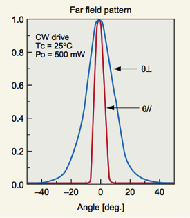
Fig. 1.13.3. A beam divergence of laser diode
Slope Efficiency
This means the proportionality coefficient of the laser output power to input currents. The unit is W/A.
This laser diode shows 1.0 mW/mA.
Monitor Current
This means a current flowing through the PD (Photo Diode), which is included in the package. PD is included in the package in order to monitor the laser output power. This laser diode has 0.7 mA in PD with laser output power of 500 mW.
Reference and Links
[1] Sony
2. Package of Laser Diode
2.1. About package of Laser Diode
The laser diode itself is a semiconductor chip, electric wires and electrodes. However commercially available laser diode are in a metal casing. This is due to the semiconductor device being weak to heat. Oscillation efficiency of the laser diode is higher compared to other lasers, but there is still energy that is not turned in to light, which becomes heat. In order to protect the semiconductor device from its own heat by dispatching it, laser diode are sold in metal packaging. Below shows, Thorlabs, inc. company’s typical laser diode packages. More information will be explained in the package description page.
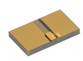
Fig. 2.1.1. Chip on Submount (COS)
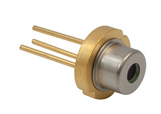
Fig. 2.1.2. TO-Can
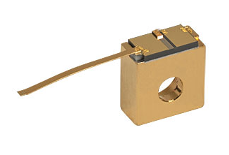
Fig. 2.1.3. C-Mount
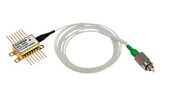
Fig. 2.1.4. 14-Pin Butterfly Mount
LD and LED are a similar light-emitting device using semiconductors. However, since LD’s output is higher than the LED’s, it is impossible to use a lens made of epoxy resin for the LD (the LED does), so the appearance of the package is very different.
2.2. TO-CAN package of Laser Diode
The most popular package of the laser diode is the TO-Can package in the Fig. 2.1.2. The TO-Can package has various diameters.
The TO-Can has three pins. Two are the cathode and the anode of the laser diode chip. The remaining one is a cathode for the output monitoring. The top of the silver cylinder is the output window, the laser light is emitted from here. At the golden base part, it is possible to attach the radiating plate. The following is a video that shows how the laser is emitted from the laser diode of a TO-Can package.
Pin placement of a TO-Can package
There are various types pin placement points of a TO-Can package, as shown billow (Quoted from Thorlabs, Inc. web site). You’ll have to conform to the pin arrangement when you connect them.
![]()
Fig. 2.2.1. TO-Can pin alignment
2.3. Fiber-Coupled package of Laser Diode
Normal LDs of today used as an excitation light source are modulated and connected to an optical fiber, as shown in the Fig. Most commonly used LD for fiber lasers and optical amplifiers is 14-pin butterfly package.
A typical 14-pin butterfly package is a single emitter type, which consists of a LD chip, optical isolator, Thermoelectric Cooler:TEC [1], and Photo Diode:PD for Laser beam monitoring (Wavelength or output monitor), and is outputted by a optical fiber attached to the ferrule.
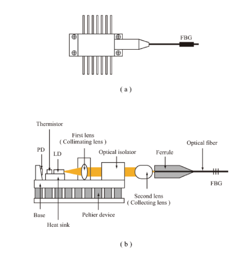
Fig. 2.3.1. The (a)appearance (with FBG) and (b) package content of a 14-pin butterfly package’s fiber pigtail.
The LD is sub-mounted to a Peltier device (TEC) for temperature control purpose. The laser outputted from the LD is focused into the optical fiber (single-mode, multi-mode, polarization-maintaining, large-diameter fiber etc.) by a micro lens. If there is a monitor PD (here a PIN Diode:p-intrinsic-n Photo Diode[2]), output can be monitored. After precise alignment they are fixed by YAG laser welding. Table shows the fiber pigtail LD used as excitation LD for fiber lasers [6-9]. A single-mode fiber: SMF pigtail LD can be fused with a SMF optic fiber, and mainly used for exciting rare-earth-doped SMF. A multi-mode fiber: SMF pigtail LD can be fused with the excitation port of an excitation combiner, and used mainly for exciting double-clad fiber: DCF.
Table 2.3.1. Fiber pigtail LD used as excitation LD for fiber lasers.
| LD type | Fiber type | Core diameter | Maximum output @CW | Reference |
| Single emitter type | SM | ~10 μm | 0.8 W | [3] |
| MMF | ~100 μm | ~25 W | [4] | |
| Bar type | MMF | ~100 μm | ~30 W | [5] |
| Stack type | MMF | ~600 μm | ~400 W | [6] |
Reference and Links
[1] TEC Microsystems GmbH,“Inside a Butterfly – Miniature Thermoelectric Coolers for Telecom Applications ” (2009).
[2] B.Doherty, M.Watertown,“PIN Diode Fundamentals,”MicroNotes Series 701.
[3] 3S PHOTONICS S.A., 1999 CHP:Up to 750mW Kink-Free, FBG Stabi- lized 980nm Pump Laser Module datasheet.
[4] Oclaro Inc., BMU25-9xx-01/02-R:25W 9xxnm Uncooled Multimode Laser Diode Module datasheet.
[5] Hamamatsu Photonics “High-power Laser Diode Bar Module”.
[6] JENOPTIK Laser diode GmbH, JOLD-250-CAXF-6P2:Fiber-Coupled Diode Laser Stacks datasheet.
3. Category of Laser Diode
3.1. FP Laser Diode
Laser oscillators are made of laser gain mediums and resonators. Resonator of a laser diode is a Fabry-Perot resonator, and in this the cleavage plane plays the role of a plane mirror.
In a crystal, atoms are periodically arranged, where the atomic force is strong and weak can be clearly distinguished. If you put a scratch in the specific place where the atomic force is weak in the crystal, the crystal cracks along the direction of the scratch. This is called a cleavage, and a surface made of a cleavage is called a cleavage plane. Laser light is reflected or transmitted through the cleavage plane, the reflectance depends on the material of the active layer. Because of this the laser diode, immediately after the cleavage is made, the cleavage plane’s reflectance becomes the same with the side where the laser light is emitted from and the opposite side. So in reality, the surface that emits light is subjected to low-reflection coating, and the opposite side is subjected to a high reflection coating. The coating is very important also to protect the surface.
3.2. DFB Laser Diode
Distributed Feedback : DFB laser diode is a mode-hop-free single longitudinal mode (single-mode) laser that has a diffraction grating structure (a wavy structure) inside the resonator. Diffraction grating structure is formed on top of the active layer (The boundary of the cladding layer and the active layer has a diffraction grating pattern). In a DFB laser, out of the light generated in the photoactive layer, only the light that has been affected by the diffraction grating comes back in to the resonator (feedback). Because only this specific wavelength light that has been selected by the diffraction grating structure strengthening, it single-mode oscillates. Because diffraction gratings are distributed along the resonance direction of the active layer, it is called a Distributed Feedback laser.
The clip bellow explains DFB laser in three minutes.
Characteristics of DFB laser diodes
Laser diodes constructed of normal Fabry-Perot resonator structure, easily multi-mode oscillates (Multi-mode oscillation becomes remarkable when in pulsed operation), oscillation wavelength changes with the environmental temperature or injection current. On the other hand with DFB lasers, wavelength stability is very high, it single-mode oscillates and line width is very narrow. Unlike Fabry-Perot semi-conductor lasers it stays single mode even in high-speed modulation (stays single mode even in pulsed operation), it is used for high-capacity, long-distance optical communication. Applications that are not optical communication are, fiber Inspection, raman spectroscopy, wavelength conversion, and sensors.
Mainly DFB lasers are supplied as Coaxial Pigtailed package, 14 Pin Butterfly package and TO-CAN package (there are also Bare Die).
The normal oscillation wavelength of a DFB laser is 760 ~ 2300 nm. In recent years nanoplus manufactures and sales DFB laser with a wavelength of 3〜6 um. Output power depends on the wavelength, however usually manufacturers sell ones that is between a few mW and 150 mW.
In addition, DFB lasers can be tuned in a range of < 5 nm without mode hop, by change the pitch of the diffraction grating or by controlling the drive current and temperature. This is the biggest difference to DBR lasers and External cavity lasers which are also single mode lasers.
3.3. DBR Laser Diode
A Distributed Bragg Reflector: DBR is a laser diode that has a diffraction grating structure at the Fabry-Perot laser’s extension of the waveguide of the active layer. In a diffraction grating only a certain wavelength (one mode) is reflected in the active layer’s direction, other light doesn’t return to it. Because of this DBR laser diodes become a single mode laser that only oscillates a single wavelength.
Below is a illustration explaining the structure of External cavity laser diode, DFB laser diode, and DBR laser diodes.
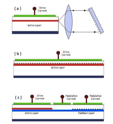
Fig. 3.3.1. (a) external cavity laser (Littrow), (b) DFB lasers, (c) DBR laser
Between the DBR laser diodes active layer and feedback layer is the phase section. By controlling the phase in this area, you can aim and control only the phase. Because this is passible, a DBR laser diode can be single wavelength operated over a wide range.
DBR laser and DFB laser
DFB laser diode is mode-hop-free, DBR laser diode is not mode-hop-free. However, the tuning range of the DBR laser diode is wider than the DFB laser diode.
Reference and Links
[1] Linglin Jiang,”High-Power DBR Laser Diodes Grown in a Single Epitaxial Step,” Proc. of SPIE Vol. 7320 (2009)
[2] Photodigm, Wavelength Tuning of Distributed Bragg Reflector Lasers
[3] R. Victor Jones,”Injection Lasers”(2000)
3.4. External Cavity Laser Diode
External Cavity Laser Diode: ECL is a laser diode with a diffraction grating (or a mirror and a diffraction grating) installed on the outside of a normal free-space output-type gain chip (AR coating laser diode). In this AR coating is applied to the cleaved surface of the gain chip’s exit side (=entrance side of the diffraction grating).
Laser emitted from the gain chip is incidents to the diffraction grating after being collimated. In the diffraction grating, all the modes incident into the gain chip is diffracted in the diffraction angle corresponding to the each mode. At this moment, one mode that has been selected by the diffraction grating goes back (is fed back) to the gain chip. With this mode resonating in the gain chip the output becomes single mode.
3.4.1. Littman type and Littrow type laser diode
There are two types in ECL, Littman type and Littrow type laser diode.
The Littman type laser diode feed backs the first-order diffracted light in to the gain chip by reflecting it with a mirror. Because the laser is diffracted twice by the diffraction grating the output level is limited.
The Littrow type laser diode feed backs the first-order diffracted light in to the gain chip directly, and takes out the laser as 0-order diffracted light. Because the laser is diffracted only once the output level is higher than the Littman type laser diode.
Also for the Littrow type laser diode, it is possible to apply a normal Fabry-Perot lasers diode that have no AR coating on the diffraction grating’s side. Because of this it is possible to make it wideband, high output, and low price.
The fig bellow is a conceptual diagram of the Littman type laser diode and the Littrow type laser diode that Thorlabs manufactures and sales. Thorlabs manufactures and sales external cavity tunable laser of 770, 1050, 1220, 1310, 1450, 1550, and 1900 nm.
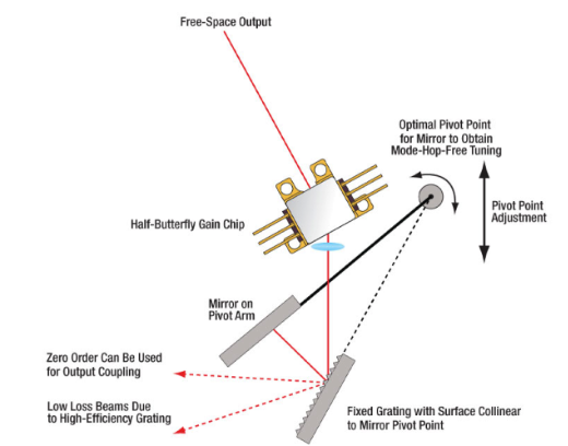
Fig. 3.4.1. Littman type laser laser diode
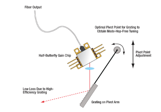
Fig. 3.4.2. Littrow laser laser diode
Characteristics of external cavity laser diode
With external cavity laser diode the design of the optical system enables a broadband tuning of more than 100 nm. The Littrow type laser diode tunes the wavelength by rotating the diffraction grating, and the Littman type laser diode tunes the wavelength by rotating the mirror.
An external cavity laser oscillates at the same wavelength band as a normal laser diode. In other words it can oscillate at a wavelength of under 630 nm, which DFB laser diode and DBR laser diode cannot.
The main factors that determine the line width of an external cavity laser laser diode are, electrical noise, acoustic noise and vibration. Considering from the structure the compact and robust Littrow type laser diode has its advantageous, however, with the Littman type laser diode it easily becomes a narrow line width due to the light passing through the diffraction grating twice.
References and Links
[1] Tholabs, inc., Tunable Lasers: Prealigned Littrow and Littman Kits
3.4.2. Fiber Bragg Grating
In amongst the 14 Pin Butterfly package laser diodes, for wavelength stabilization, have Fiber Bragg Grating written in the pigtail fiber. The light emitted from the gain chip is coupled to a pigtail fiber, and by the FBG the wavelength corresponding to the reflection band of the FBG returns (is fed back) to the gain chip. As a result, the light of reflection wavelength of the FBG gain chip resonates selectively obtaining a narrow spectral width laser.
Characteristics of the FBG with fiber pigtail type laser diode
FBG with fiber pigtail type laser diode’s spectral width is about 0.5 ~ 1 nm, and the spectral shift with temperature is about 0.01 nm / deg. From 3SP Group a 1050 mW(Kink-free) model is available. Compared to DFB laser diode and DBR laser diode , the spectral width is wide, but it can cope with high output. Because of this products of 976 nm wavelength is often used as excitation light source for fiber lasers.
3.5. Quantum Dot Laser Diode
The quantum dot is fine particles composed of a oxide semiconductor or compound semiconductor, consisting of 10 to 50 atoms. Quantum dot laser diode is a type of laser diode with quantum dots spread over the active layer. There are three types of structures of a semiconductor with the name “quantum” attached to it, quantum well, quantum wire and quantum dot. Quantum well is those that have an active layer thickness of about 10 nm. Quantum wire’s active layer is a thin thread. Make that thread short, makes it a quantum dot. The video below explains quantum wells, quantum wires, quantum dots.
By controlling the size of the quantum dot, it is possible to control the emission wavelength. The strong point of quantum dot laser diodes are: low power consumption, high efficiency, and temperature dependence being very low. From these features, adjustment of the modulation current and bias current is not required for the quantum dot laser diode. As for the usage for quantum dot laser diode, optical communication is most promising. Note here that, there are LED, SLD, and SOA using quantum dots are also commercially available.
Videos explaining quantum dot laser diodes
3.6. Quantum Cascade Laser Diode
Carriers in a laser diodes are usually electrons and holes. It emits by recombination of holes in the valence band and electrons in the conduction band. On the other hand, quantum cascade laser diode, semiconductor quantum wells are connected in multiple stages. It is a type of laser diode, using the transition between sub-bands. Carriers in the semiconductor is one type. Emission wavelength due to band-to-band transition depends on the energy band gap of the semiconductor materials. The size of the inter-sub-band-energy can be changed by changing the width of the quantum well, so emission wavelength can be flexibly designed. Oscillation region of quantum cascade laser is mid-infrared to terahertz band. At room temperature, output of 20 mW has been done.
Below is a video that Alpes Lasers, Inc. has published, showing how the quantum cascade laser oscillates.
3.7. VCSEL
VCSEL emits the laser light perpendicular to the substrate surface, while normal laser light from laser diode is emitted from the semiconductor’s cleavage plane. Below is a video explaining VCSEL.
Manufacturing process
VCSEL does not need to have the semiconductor facet cleaved, and manufacturing of the VCSEL chip can be carried out in one go on the wafer, making it suitable for mass production, thus lowering the price. Also inspection can be done while it is still a chip.
Performance
Performance wise, its oscillation threshold current is under mA, has low power consumption, and is not suitable for high power applications. This is due to the active region being short. Output of one VCSEL basic element is a few mW, by arraying several hundred basic elements it is possible to output more than 1 W. This sort of VCSEL packages are commercially available. Emission light is not elliptical cone shape as an edge-emitting laser, but conical. Allowing high-density array is also a great feature. Important parameters of VCSEL are: Linewidth, Bias Current, Data Rate, Contact Configuration, and Channel Configuration.
Usage
VCSEL from being mass-produced in 1994, is used in a wide range of applications such as: Sensing, Optical interconnects, Laser printer, Bar code reader, Computer mouse, and Light Peak. A famous maker is II-VI Laser Enterprise. They have MOCVD and CVD suited for mass production.
4. Parameters of Laser Diode
4.1. Monitor Current
TO-CAN and 14 pin butterfly type package has a photo diode incorporated. The photo diode generates a current in accordance with the intensity of the laser emitted from laser diode. Meaning, by monitoring the current generated by the photo diode, it is possible to monitor the output power of the laser diode. By feeding back the situation to the temperature control element (because laser diodes are temperature-dependent), it is possible to control the laser output power. Amount of current generated at a standard output is on the laser diode’s data sheet.
4.2. Reverse Voltage
In the specification documents of a laser diode, reverse voltage and forward voltage is described. This is the reverse voltage that must not be applied to the laser diode. If applied the laser diode will be destroyed. In order to prevent the laser diode being destroyed, it must have a protection circuit. In reverse voltages, there are PD reverse voltage and laser diode reverse voltage.
4.3. Operating Temperature and Storage Temperature
Operating temperature
Laser diodes must be used in a temperature controlled state. Operating temperatures are described in the data sheet of the laser diode. Operating temperature of a typical laser diode is -20 ~ 50 °C. The various parameters on the data sheet is when operated at 25 °C.
Storage temperature
Storage temperature is the temperature that should be kept when a laser diode is not operated. It is usually about -40 ~ 80 °C. The range is wider than the operating temperature.
4.4. Slope Efficiency and Quantum Efficiency
External quantum efficiency and internal quantum efficiency
Quantum efficiency is the probability of a photon being obtained from a transition of an electron. The internal quantum efficiency is quantum efficiency considering the loss within the resonator. The external quantum efficiency is quantum efficiency that takes into account the loss caused by the outside parts of the laser diode body.
Differential quantum efficiency
Differential quantum efficiency is the quantum efficiency obtained from the change in the number of photons (ΔPop) within the changes in the current flowing in the semiconductor (ΔI). Differential quantum efficiency is constant at the threshold current and over. Differential quantum efficiency can be determined from the slope efficiency as introduced below.
Slope efficiency
Slope efficiency is the increases percentage of the light output proportional to the current, when a threshold current is injected. That is to say, slope efficiency is the slope of output light – injected current curve (LI curve) of the laser diode. The unit is W / A or mW / mA, it is sometimes written in the specifications of the laser diode.
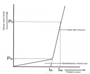
Fig. 4.4.1. Output light – injected current curve.
4.5. Oscillation Threshold
Unlike the LED, a laser diode is a laser with a resonator, so it has a resonating threshold current. Figure 4.4.1. is a diagram showing the output light – injected current characteristic. When current is between 0 ~ IthA spontaneous emission light is emitted from the laser diode. The spectrum at this time is broad, like a LED. When the current exceeds the Ith, laser oscillation occurs. At this time, the spectrum becomes narrow, almost one wavelength. When it is current > Ith, output light increases in proportion to the current. The video below illustrates how the laser oscillates.
4.6. Optical Output Power
Unit of light output of the laser diode is watt, the same as other lasers. Units of the brightness of LED, which is often compared to laser diode, is also watts. However, LED’s watt shows the power consumption of the LED. It is a display for inferring the brightness by the power consumed. In laser diode, the electrical energy is converted to light, because of this luminous efficiency of the laser diode can be easily obtained. Efficiency(%) = Optical output power / ( Operating voltage x Operating current )
4.7. Direct modulation
The method of modulating light intensity by modulating the injection current of a laser diode is called direct modulation. With this frequency chirping occurs. Because of this, the spectrum gets wider than the spectral broadening due to the modulation, strongly affects the wavelength dispersion of the optical fiber. With the use of an external modulator, it is possible to avoid this effect, because the laser diode light source can be driven with a steady current.
The types of external modulators are, Electro-optic effect type (EO), Photo acoustic effect type (AO), and the Electro-absorption type(EA) that uses the absorption effect.
Among the EO modulator, the lithium niobate (LiNbO3, LN) waveguide types are called LN modulators.
4.8. Beam Spread of Lasers Diodes
The laser beam of laser diode spreads in an elliptical cone shape. The shape of the beam of a laser diode near the output end and a few cm from the output end is different. The pattern of the beam near the output end is called Near Field Pattern (NFP). The beam pattern a few cm away from the output end is called Far Field Pattern (FFP).
The figure below shows NFP and FFP.
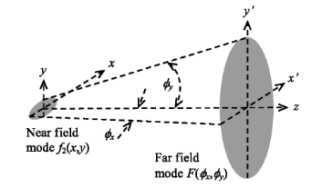
Fig. 4.7.1. NFP and FFP
Quote from: SPIE Digital Library:Modeling the near-field and far-field modes of single spatical mode laser diode
Near the laser diode facet, the laser is a horizontal oval shape in the x-axis direction, but in FFP, the ellipse is horizontal in the y-axis direction. This is, because the outlet is narrower on the y-axis direction, compared to the light that comes out of the x-axis direction, thus causing it to diffract largely.
FFP
In the data sheet of the laser diode, FFP is represented by θ// and θ⊥. θ// indicates the angle at which the laser diode spreads laterally, and θ⊥ indicates the angle that extends in the vertical direction. The angle is defined in FWHM, which is when the intensity of the laser beam is 1/2 of the central portion of the laser beam. Usually, θ// is 8 ° and θ⊥ is 30 °, so the laser extends in the vertical direction.
5. Application of Laser Diode
5.1. Application to Fiber laser of laser diode
Fiber laser oscillator is composed of pump laser diode and active fiber as shown in figure.
Fiber laser amplifier is composed of signal laser, pump laser diode and active fiber as shown in figure.
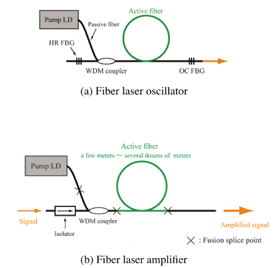
Fig. 5.1.1. (a) Fiber laser oscillator and (b) Fiber laser amplifier
Laser diodes are used as pump laser and/or signal (seed) laser in fiber lasers.
Active fiber can be divided into two types single-clad fiber (SCF) and double-clad fiber (DCF).
Laser diode used in fiber lasers are shown in the table.
・ Laser diode used as pump-laser of single-clad fiber
・ Laser diode used as pump-laser of double-clad fiber
・ Laser diode used as seed-laser of fiber laser amplifier
Table 5.1.1. Pump-laser of single-clad fiber
| Perpose | Kind of fibers |
Doped rare earth |
Wavelength of laser diode(nm) |
Polarization maintaining |
Fiber Bragg grating |
Isolator | Recommended manufacturers |
| Pumpimg | Single clad | Tm | 793 | ○ | ○ | Lumics | |
| Yb or Er:Yb | 976 | ○ | ○ | 3SP Group | |||
| OPTOENERGY | |||||||
| Er | 976 | ○ | ○ | 3SP Group | |||
| OPTOENERGY | |||||||
| 980 | ○ | ○ | 3SP Group | ||||
| ○ | ○ | Fitel | |||||
| ○ | ○ | Fitel | |||||
| 1480 | ○ | ○ | Fitel | ||||
| ○ | ○ | Fitel |
Table 5.1.2. Pump-laser of double-clad fiber
| Use | Kind of fibers |
Doped rare earth |
Wavelength of laser diode(nm) |
> 100 W | Volume Bragg grating |
Feedback protection |
Recommended manufacturers |
| Pumping | Double clad | Tm | 793 | ○ | DILAS | ||
| Lumics | |||||||
| Yb or Er:Yb | 915 | ○ | DILAS | ||||
| Jenoptik | |||||||
| 940 | ○ | OPTOENERGY | |||||
| 976 | |||||||
| Er | 976 | ○ | ○ | BWT Beijing | |||
| 980 |
Table 5.1.3. Seed-laser of fiber laser amplifier
| Use | Kind of fibers | Wavelength of laser diode(nm) | Recommended manufacturer |
| Seed | Tm Fiber Laser | 2000 | Elbana Photonics |
| Yb Fiber Laser | 1064 | 3SP Group Innolume Lumics SHIMADZU QD Laser Onefive |
|
| Er or Er:Yb Fiber Laser | 1550 | Onefive |
Active fiber is the fiber that rare earth element such as Er, Yb, Nd, Pr, Tm and Ho is doped.
The wavelength of laser in laser diode varies depending on the semiconductor-composing element as shown in table. And rare-earth-doped fiber pumped in wavelength range of each laser diode is shown in table.
Laser diode can be used for broad wavelength range.
Laser diode is most important element to develop high-power fiber laser.
Table 5.1.4. Wavelength of each semiconductor-composing element and kinds of rare-earth-doped fiber to be pumped
| semiconductor-composing element | wavelength[μm] | rare earth |
| InGaN/GaN | 0.38-0.48 | Pr |
| GaAs/AlGaAs | 0.78-0.86 | Nd, Tm |
| InGaAs/GaInAsP/GaInP | 0.9-0.98 | Yb, Er |
| GaInAsP/InP, AlGaInAs/InP | 1.47-1.6 | Er |
| InGaAsP | 1.8-1.96 | Ho |
5.2. Application to DPSS laser of laser diode
Laser diodes are usually used as the pump-laser in the DPSS (diode pumped solid-state) laser.
Laser oscillator consists of a laser medium and its pump source.
As the pump source, flash lamps and laser diodes are usually used.
Flash lamp
Flash lamp is a cost effective source and it offers high output power. We must be careful a large heat load for the laser medium. This is because the flash lamp has a broad spectrum so that a large part of the optical energy transfers to heat energy.
Laser diode
According to the development of high power, high efficiency, and long life laser diodes (LD’s) in 1980s, the technology of solid-state lasers pumped by laser diodes has been developed. Since the emission spectrum of LD’s is narrow, high absorption efficiency can be easily achieved. Furthermore, high-density excitation can be achieved because of its high coherence of the output beams.
DPSS lasers are excited in the way as shown in Fig. 5.2.1. Figure 5.2.1. (a) shows the LD side-pumped system and (b) shows the LD end-pumped system.
Q-switch laser or Mode-locked laser is achieved by inserting some optical elements in the laser cavity. For the high-power DPSS laser, cooling system using air or water is necessary.
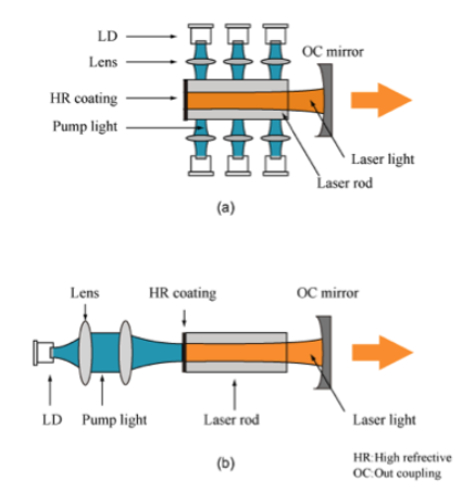
Fig. 5.2.1. Excitation method for the solid-state laser.
(a) LD side-pumped system, (b) LD end-pumped system
5.3. Application to Material Processing of laser diode
The Properties of Laser Sources for Material Processing
The features and types of laser sources for material processing are shown in a following table.
Table 5.3.1. The features of laser sources for processing
| Medium | Wavelength (nm) |
Oscillation form | Max output | Efficiency | Type of process | |
| Gas | CO2 | 10600 | CW Pulse (1 Hz〜a few hundred kHz) |
A few dozen 10 W (CW) |
8% | Cuting Microfabrication |
| TEA-CO2 | Gas pressure dependence | Pulse | A few dozenW | Cuting | ||
| Excimer | ArF | 193 | Pulse (1 Hz〜1 kHz) |
a few hundredW | Microfabrication | |
| KrF | 248 | |||||
| XeCl | 308 | |||||
| Solid (Crystal) |
YAG | 1030 1064 |
CW Pulse |
A few dozenkW (Disk, CW) |
〜20 % @Rod 〜25 % @Disk |
Cuting Welding Carving |
| YVO4 | 1064 | Pulse (1 Hz〜a few hundred kHz) |
A few kW | Cuting | ||
| Ti:Sapphire | 800 | Ultrashort Pulse (1 Hz〜100 MHz) |
A few dozen W | Microfabrication | ||
| Fiber | Yb fiber | 1064 | CW Q switch Ultrashort Pulse (A few dozen kHz〜100 MHz) |
A few dozenkW (CW) | 〜35 % | Cuting Welding Marking Microfabrication |
| Laser diode | Semiconductor | < 980 | CW Pulse (1 Hz〜1 kHz) |
A few kW | 〜60 % | Cuting Welding |
CO2 laser
CO2 lasers are widely used in laser processing owing to its low cost and high beam quality. This laser will be continued to use in laser processing.
YAG laser
Although the beam quality of the LD pumped YAG laser is relatively low, this laser offers another advantages such as high efficiency of the high harmonic generation. Previously the lamp excited YAG laser are used, but now such lasers are not used owing to its low lasing efficiency and low beam quality.
Yb fiber laser
Yb fiber lasers are advantageous in the beam quality with respect to that of LD’s. However, the initial cost is higher than the LD’s.
Direct laser diode system
Direct laser diode system offers very compact and low cost. However the beam quality of laser diodes is intrinsically lower than fiber lasers.
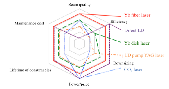
Fig. 5.3.1. Comparison of lasers for material processing
Laser surface processing
Laser surface processing is one of the laser processing techniques. The laser beams are used for surface reforming through the laser irradiation to the material surface. The laser surface processing includes heating, melting, and evaporating process. The heating process deals with surface quenching and annealing. The melting process deals with alloying, build-up welding, and grazing. The evaluating process deals with impact effect in the material and drying process. In the surface processing, a CO2 laser, a Nd:YAG laser, a laser diode, and a fiber laser are used as for a laser source.
5.4. Application to Telecom of laser diode
5.4.1. History of Telecom
In 1970 both low loss (20 dB/km) of silica-based optical fiber and laser diode operation at room temperature was achieved this was the first step for practical use of telecom. Since then, laser diode development has been made for telecom to achieve higher-speed and longer-distance transmission.
In the early stage, laser diode with wavelength of 0.8 μm and multi-mode fiber were used for optical fiber telecommunication. After this, band frequency with low data transmission loss has been shifted to a longer wavelength of 1.3 μm or 1.55 μm band have started being used. Also, single mode fiber (SMF) has begun to be used in long-distance transmission in order to remove the influence of transmission-velocity difference in the transverse-mode.
Since the theoretical limit of transmission loss (<0.2 dB/km) for optical fibers was achieved in the 1.55 μm band, the band has been used for long-distance trunk. With the 1.55 μm band influence from optical-fiber dispersion needs to be considered. The spectrum of laser lights widen as modulation speeds up. Long-distance transmission causes the disorder of high-speed signal leading to limitation of transmission distance. In order to avoid the disorder distributed feedback (DFB) laser diode was studied and commercialized, which can achieve narrow spectrum regardless of modulation.
With the development of erbium-doped fiber amplifier (EDFA), the frequency change (chirp) due to high-speed modulation of laser diode had become the cause of limitation in the transmission distance. In order to avoid the problem the method of modulation by an external modulator was suggested. There are two types of external modulations: one which uses a LiNbO3 crystal and one which uses a compound semiconductor crystal. High-speed operation has been achieved by DFB laser integrated with electro-absorption (EA) modulator.
Optical fiber amplification technology was born in the late 1980s. It has made great revolution in telecom technology by achieving non-relay long-distance transmission. In optical fiber amplifiers there are the method of pumping doped rare-earth ion and the method of using Raman amplification. In these methods 0.98 μm or 1.4 μm band laser diode are used. It enables capturing the wavelength as the optical signal channel. The development of wavelength-tunable laser diode which changes the oscillation wavelength by about 30 nm has attracted attention.
5.4.2. Basic Structure
Briefly speaking, laser diodes are diodes which emit light when injected with a current. In telecom, 1.3 μm and 1.55 μm band laser diodes are used and the light emission can be obtained by injecting forward bias current to an active layer. By using the active layer that is sandwiched by crystals with a wider-band gap, career (electrons and holes) is confined into the active layer and the emission efficiency increases. Refractive index of the active layer is slightly higher than the surrounding semiconductor crystal and the waveguide is made along the active layer. In the case of a Fabry-Perot (FP) laser diode cleavage surface of the crystal becomes the mirror of the resonator. It causes stimulated emission in the active layer achieving laser oscillation. DFB laser has different structure from FP laser and the resonator structure is composed of diffraction grating engraved in vicinity of the active layer.
Optical signals are generated by modulation of the current magnitude injected in to the laser diode. This method is called direct modulation. Direct modulation method and external modulation method are shown in table 5.4.1. Integrated laser diode has both EA modulator and DFB laser diode on the same device that adopted external modulation. Optical signal from the DFB laser diode is guided into the EA modulator that can absorb the signal upon applying reverse bias voltage. Since career density fluctuation inside the active layer is smaller compared to direct modulation external modulation can suppress the chirp. Therefore, external modulation method can achieve high-speed modulation with low spectrum disorder caused by the dispersion.
Table 5.4.1. Comparison between direct modulation and external modulation
| System | Direct modulation |
External modulation | |||
| Laser | Optical Modulator + Integrated Laser | Optical Modulator + Laser | |||
| Structure | Constitution | Integrated | Integrated | Separate or Hybrid Integrated |
|
| Light source | Longitudinal mode control |
DFB | DFB | DFB | |
| Transverse mode control | BH | BH (ridge) | BH | ||
| Active layer material | InGaAsP-MQW | InGaAsP-MQW | InGaAsP | ||
| Modulator | Modulation principle | Quantum-confined Stark effect electro-absorption |
EO effect MZ interference |
||
| Transverse mode control | BH (ridge) | Diffused waveguide, others | |||
| Material | InGaAsP-MQW | LN (GaAs) | |||
| Characteristics | Modulation bandwidth [GHz] | ~20 | >40 | >30 | |
| Chirp index | 2~3 | ~0.25 | -1, 0, 1 | ||
Active layer structure
When laser diode was first commercialized thin-film crystal was used as an active layer. Recently, multiple quantum well (MQW) is used for the active layer. Quantum well means that crystal with is about 10 nm thick is sandwiched by crystals with wider band gap and multi quantum well creating a MQW. Threshold current density for oscillation of the quantum-well structure is only a fraction of other structures.
The first prototype of the quantum well laser diode using GaAlAs related materials was reported in year 1975. Since it was found that the laser diode has one-third of the current density threshold (0.25 kA/cm2) compared to DH laser much research has been performed. It started to be used for laser diodes for telecom after InGaAsP related quantum well structure was made by metal organic chemical vapor deposition.
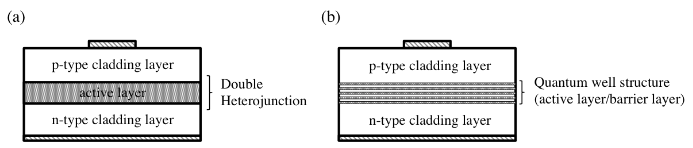
Fig. 5.4.1. Active layer structure. (a) double hetero structure and (b) MQW.
Control of transverse mode
Control of transverse mode of laser diode has two types (Fig. 5.4.2):
Method-A:Gain-guiding type structure controlling the gain depending on the place.
Method-B:Refractive index-guiding type structure controlling by refractive index difference of the crystal
Method-A confines oscillation light by using the phenomenon where current density becomes high directly under the electrode to inject current. Method-B confines oscillation light by making waveguide through refractive index difference between different crystals. Since method-B can make stable waveguide even if career density decreases inside the active layer with increasing light density in the resonator. Because of this it can be used for many types of laser diodes including telecom.
In refractive index-guiding type structure, the type with a stripe active layer buried into a crystal is called buried hetero (BH) type. In InGaAsP related laser diode because threshold current value largely depends on the temperature, BH structure which conducts operating current to active layer are used in many cases. Active layer width is designed to meet cut-off condition of high-order mode. This is about 1~2.5 μm. Also, in some cases ridge structure is adopted. Ridge structure is used for high-speed device since the structure can be achieved low volume easily and can be easily used for laser structure even for InGaAlAs related crystals relatively susceptible to oxidation.
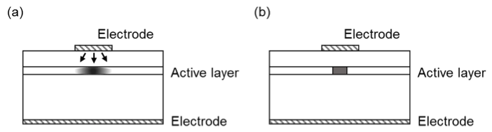
Fig. 5.4.2. Control of transverse mode of laser diodes.
(a) gain-guiding type structure and (b) refractive index-guiding type structure.
Control of longitudinal mode
In optical fibers propagation constant which is decided by glass material and structure has wavelength dependence. Therefore, if laser diode with multi mode is used as the source spectrum is disordered by dispersion characteristics and propagation distance is limited. In order to avoid the problem DFB laser diode is used. With DFB laser diode longitudinal mode can be selected by diffraction grating in active layer. Consequently, DFB laser diode can be operated with single-longitudinal mode even with career density fluctuation in active layer with high-speed modulation. To create a diffraction grating a two-beam interferometry by an Ar laser or electron-beam lithography is used.
In order to enhance the selectiveness of longitudinal mode, phase-shift DFB laser and gain-coupling DFB laser were developed. Both phase-shift and gain-coupling DFB laser achieve stable and single longitudinal mode operation by adjusting reflected-light phase inside the resonator. The phase shift DFB laser adjusts the light phase by reversing grating period of diffraction grating in the resonator. The gain coupling DFB laser adjusts the light phase by engraving diffraction grating directly in the active layer and giving the gain a cycle.
Since GaAsP related semiconductor crystal mainly used for telecom is not susceptible to oxidation. Diffraction grating can be engraved on or in the vicinity of the active layer. With distributed Bragg reflector (DBR) laser diode, longitudinal mode is selected also by diffraction grating as well as DFB laser diode. DBR laser diode has structure of integrated diffraction grating outside the active layer. It was originally developed as the light source for coherent telecom and now it is one of the types of tunable laser diodes.
5.4.3. Various Laser Diodes Used for Telecom
In the telecom field 1.3 μm and 1.55 μm band laser diodes are used as main light source since silica fiber lasers have less transmission loss in the band. Additionally, laser diode with different band are used for pumping source for optical amplification or for short-distance optical link. Here are introduced various laser diodes used for telecom. In table 5.4.2, laser-diode modules are introduced in each wavelength bands.
0.8 μm
This is used for datalink combined with multi-mode fiber. Particularly, it has started to be used as a light source for short-distance data transmission such as gigabit ethernet by using VCSEL (vertical cavity surface emitting laser).
0.98 μm
This is used to pump EDFA used for optical signal amplification in the 1.55 μm band. Light excitation in this band can make optical amplification with low noise factor. It is used for pre-amplification at a receiver or for forward pumping at repeaters.
1.3 μm
FL type is used as light source for FTTH (fiber to the home), for subscriber line under 150 Mbit/s, as light source for office line up to 2.5 Gbit/s or for datalink. DFB laser diode is used for branch line or datalink, or analog-modulated laser (used for cable television). It is also used for pulse-light source for OTDR (optical time domain reflectance) designed for maintenance and inspection of optical fiber transmission line.
1.4 μm
This is mainly used as pumping excitation light source for EDFA. Because it is a wavelength close to 1.55 μm, it has a high energy conversion efficiency. Compared to 0.98 μm band, it is suitable for higher output power and can be used for high-output EDFA by backward pumping. Also, it can be used as pumping light source for Raman amplifier, which achieves signal amplification by induced Raman scattering.
1.5 μm
Because it is in the low loss band of optical fiber it is used for long-distance light source such as trunk. Because this band is highly influenced by dispersion of the optical fiber, DFB lasers which work with single longitudinal mode are mainly used. Main use is for research and development. small-lot production.
Table 5.4.2. Various laser diodes for telecommunication
| Wavelength[μm] | Structure | Material | Substrate crystal | Output[mW] | Use | |
| longitudinal mode | transverse mode | |||||
| 0.85 | VCSEL | GaAlAs | GaAs | 1 | data link (~10 Gbit/s/ch) | |
| 0.98 | FP | BH(ridge) | InGaAs /AlGaAs |
~500 | pumping source for EDFA (1.5 μm band) | |
| 1 | pumping source for EDFA *(1.3 μm band) | |||||
| 1.06 | pumping source for EDFA *(1.4 μm band) | |||||
| 1.31 | VCSEL* | GaInNAs | 0.5 | datalink (~2.5 Gbit/s/ch) | ||
| FP | BH(ridge) | InGaAsP InGaAlAs |
InP | 5~15 | FTTH (~155 Mbit/s), office line, datalink (~10 Gbit/s), PON (~155 Mbit/s) | |
| DFB | 5 30 300 |
branch line,datalink (10 Gbit/s) | ||||
| CATV | ||||||
| OTDR (pulse) | ||||||
| 1.48 | FP | ~500 | pumping source for EDFA | |||
| 1.4 | pumping source for Raman amplifier | |||||
| 1.55 (1.47 ~ 1.61) |
5 | FTTH (~155 Mbit/s) | ||||
| DFB | 10 50 200 |
trunk,metro,datalink (2.5 ~ 10 Gbit/s) | ||||
| light source for external modulation | ||||||
| OTDR (pulse) | ||||||
| DFB integrated with EA | 5 | trunk,metro,datalink (2.5 ~ 40 Gbit/s) | ||||
| DFB array* | 10 | metro (tunable wavelength) | ||||
| DBR* | 10 | |||||
| MEMS-VCSEL* | 1 | |||||
| OTDM* | ||||||
*for research and development, and small-lot production.
5.5. Application to Biology of laser diode
Lasers are used for wide variety of medical applications such as surgical treatments, cosmetics, and eye cares as shown in table. Basic of the laser treatment is removal of unneeded tissues and diseased tissues through the evaporation and carbonization of tissues by the illumination of a laser beam.
A surgery using a laser scalpel is most typical application. Compared with a conventional scalpel, the laser scalpel is advantageous by following reasons: i) The cut tissue is coagulated by the photothermal effect so that the procedure of stopping the flow of blood is unnecessary. This is effective to shorten surgical time. ii) The laser scalpel is sanitary because the one cut tissues without direct contact. In cosmetic treatments, the laser is used for removing moles, freckles, spots, and hairs. Recently the laser surgery for eye care including LASIK becomes popular. Types of surgical lasers include argon lasers, Nd:YAG lasers, CO2 lasers, excimer lasers and laser diodes.
Note that the misusing of lasers causes loss of eyesight and further deterioration of diseased tissue. Thus, it is important to use lasers in an appropriate manner.
Laser diodes have been used in a variety of medical applications such as PDT, Surgery (Coagulation, hemostasis-incision endoscopic), Snoring treatment Pain healing and mitigation of indirect jaw disease, Laser anesthesia, Shaping of the peri-implant gingiva, Whitening, Diagnosis of bone marrow, Hyperesthesia, Bruises, stains, freckles up, Hair loss, Headache, Whipping, Frozen shoulder, Elbow pain, Chest pain, Low back pain, Various pain such as indirect pain, Nerve paralysis, Contusion, Abrasions, Burn, and Treatment of keloid.
Table 5.5.1. Lasers for medical applications
| Diagnosis and treatment | Used laser | Use |
| Ophthalmology | Ruby laser | Laser photocoagulation, Retinal detachment, LASIK (myopia, astigmatism treatment) |
| Fiber Laser | LASIK | |
| Excimer laser (ArF) | Cornea removal, Cornea-like cut, Laser photocoagulation, Retinal detachment, LASIK | |
| Surgery | CO2laser | Laser knife, Ccancer treatment, Hay fever, Allergic rhinitis (Nasal mucosa ablation) |
| Nd:YAG | Allergic rhinitis, Endoscopic incision, hemostasis and coagulation. Snoring treatment | |
| Ar laser | Photodynamic therapy (Photodynamic treatment) | |
| Laser diode (InGaAsP) |
PDT, Surgery (Endoscopic coagulation, hemostasis and incision endoscopic), Snoring treatment | |
| Dentistry | CO2laser | Laser sealant, Treatment of hypersensitivity, Root canal treatment, Pigmentation removal, Enamel acid resistance strengthening |
| Er:YAG laser | Pyorrhea treatment, Pigmentation removal, Gum whitening, Cutting hard tissue (bones or teeth), Incision or excision of Gingiva or mucosa | |
| Nd:YAG laser | Pyorrhea treatment, Laser anesthesia, Gum whitening | |
| Ar laser | Whitening (Bleaching), Pigmentation removal, Pigmentation removal, Enamel acid resistance strengthening | |
| HeNe laser | Stomatitis treatment, Easing and treatment of pain caused by temporomandibular joint disease | |
| Laser diode | Easing and treatment of pain caused by temporomandibular joint disease, Laser anesthesia, Peri-implant gingiva shaping, Whitening, Bone marrow diagnosis, Hyperesthesia | |
| Aesthetic Plastic Dermatology |
CO2laser | Bruises, Stains and Freckles removel |
| Er:YAG laser | Scars, rosacea, tattoos, skin linear, lentigines, warts, epidermal nevus, seborrheic keratosis, senile pigment nevus, etc. | |
| Nd:YAG laser | Tattoo, blue nevus, nevus of Ota, keloid, acne, wrinkles | |
| Alexandrite Laser | Stains, Ota nevus, seborrheic keratosis, traumatic tattoo, tattoos, acne, hair removal | |
| Dye Laser | Hemangioma simplex (red bruises), stain, freckles removal | |
| Ruby Laser | Bruises, spots, freckle removal, mole, senile plaque, flat nevus, nevus of Ota | |
| Laser diode | Bruises, spots, freckle removal, hair removal | |
| Orthopedics | Laser diode (GaAlAs) |
Headache, whiplash, frozen shoulder, elbow pain, chest pain, back pain, joint pain, nerve paralysis, contusions, abrasions, burns, Keloid treatment |
5.6. Application to Laser Display and Illumination of laser diode
Laser diodes are very useful as a high-output light source because it has a larger amount of light compared to LEDs, and are possible to increase the light flux with a small number of elements. Also lasers have a high directivity. For this reason the optical design to use it as a light source is easy. Therefore, if laser diode lights are designed properly, can be made lite and compact allowing mobility. There are high expectations in use in the future.
5.6.1 Laser diode used laser display
A technique of laser display using laser diodes as its laser source is receiving a lot of attention because of following two reasons: One is the energy efficiency. Compared with other lasers, laser diodes are superior in laser efficiency. Such property is suited to today’s environment-conscious society The other is compactness. The development of compact displays is also important as well as that of the large size display. Development of much smaller device is important for the creation of a ubiquitous network society.
Concrete examples of the laser display with laser diodes are explained following sections.
5.6.2 Laser projector with laser diodes
Typically, a projector is the device for the projection a light or an image on the screen. Recently, a projector includes the device to enlarging images, which are indicating on another small display devices. In this section, such device for enlarging the images by using lenses is also defined as the projector. Laser projectors include scanning type and spatially modulation type for the projection.
Scanning type
Intensity modulated multi-color laser beams are combined collinearly. Then the beams are scanned on the screen to project an image. Projected image is recognized by using the residual image effect. Initially, a polygon mirror and a galvanometer mirror are combined and used for horizontal line scanning and vertical line scanning, respectively. But now, the angle of the mirror is mechanically controlled to wide-range scanning. Recently, micro electro mechanical systems (MEMS) are used. The scanning type laser projector can be compact and focus free because the projector lens is not needed.
Since high power laser diodes and the technology of MEMS are developed, the laser projector with scanning type recently attracts attention. There is a tradeoff between the resonant frequency and the scanning angle. To high speediness and wide scanning angle simultaneously, the development of MEMS is underway.
Example:
PicoP developed by Microvision is a scanning type laser projector for sale. Red and blue laser diodes and the SHG of the red laser diode are combined collinearly and are reflected by a MEMS scanner.
Two-dimensional spatial light modulator type
In this type, red, blue, and green laser beams are modulated by two-dimensional spatial light modulator (2D-SLM), and then these beams are combined and projected on a screen by a projection lens. There are three types of 2D-SLM: a liquid crystal display (LCD), a digital light processing (DLP), and liquid crystal on silicon (LCOS). Now, LCD and DLP are typically employed for sale.
In the LCD type, a laser beam transmits a transmission type LCD to adjust the brightness and illuminates the screen to image. In the DLP type, a laser beam illuminates on a digital micromirror device (DMD). By applying digital signal to MEMS, the laser beam is reflected to the screen for image projection. In the LCOS type, the laser beam is reflected by using LCOS for the projection.
The intensity of light in the 2D-SLM is inversely proportional to the product between the area of the light source and divergence angle. For this reason, the point source, such as a laser, is suited for the light source of the laser projector with the 2D-SLM.
Example:
Barco develops a high-intensity laser projector. Light Blue Optics develops a touch screen type laser projector, which includes an infrared sensor and a technology of holography to sense human motion.
5.6.3 Laser TV with rear-projection system
Many displays much as digital signage and flat-screen TV uses LCD backlight system and a rear projection system are widely used. Laser TVs have been developed with these systems. Principles and examples of rear-projection system using RGB3 color lasers and backlight system is stated here.
Rear-projection system uses RGB3 color laser as a back light, superimposing the image signal with a spatial light modulator, outputting the enlarged image and projecting it on to the screen from the back side of the screen by a projection lens.
There is a rear-projection system laser TV that Mitsubishi Electric has developed [1].
It replicates a wide color space with xvYCC standard using Mitsubishi Electric’s own color management technology ” Natural Color Matrix (NCM)”.
This is a system that controls the three laser diodes that make up the three primary colors of light (RGB) and the colors that are actually displayed to be faithful to the video signal. DMD is used as a spatial light modulator In 2008 the worlds first laser TV was sold in America. This TV used laser diodes for the red and blue, and used second-harmonic generation (SHG) for the green [2]. This DLP projection TV has the following features: Color reproducibility 2 times the normal LCD TV, power consumption significantly lower than LCD or plasma, thinner than the previous rear projection TVs due to the “super-wide-angle optical engine” that provides a wide projection angle.
Also, unlike SHG method, there is another method to get RGB 3 color through exciting fluorescent material by laser light. Prysm, Inc (U.S) has the technique to output the image through scanning coated RGB fluorescent material with modulating blue laser diode. This is to use greatly different optical method, but has the character not to make speckle noise.
Laser television with liquid crystal backlight system
Liquid crystal backlight system has following two methods:
(1) Edge light system to expose the light uniformly into liquid crystal through guiding the light from the side to light guide panel and using diffusion and reflection sheet.
(2) Direct under system to expose the light over all of the liquid crystal through LED array.
Display with liquid crystal backlight system can be used not only for Television, but also
for larger scale application, such as digital signage (digital signage). It is expected that high efficiency laser diode realizes large-sized screen and display with high-intensity, high-resolution, and energy saving.
5.6.4 Head-up display with a laser
Head-up display is the device that the information is imaged on the windscreen of cars and airplanes. It offers high level of safety when people is steering vehicles because there is no movement of viewpoint to see meters or navigation systems. Further enhancement of the safety can be achieved by imaging the information on to the eyes. The laser contributes the improvement of the visibility of the projected images.
The technology of the head-up display also uses in medical treatments. In drawing blood samples, by projecting the map of blood tubes on a human body makes easy to draw the blood. In image diagnosis, by projecting the results of X-ray inspection and/or computed tomographic scanning on the patient body makes easy to give a diagnosis.
Example:
Microvision and Pioneer develops a laser-projected head-up display. This is achieved by applying the technology of RGB laser scanning, which was developed by Microvision, to the projector module.
5.6.5 Wearable display
The wearable display is the display device incorporated in clothing and accessories. The glasses and hats are typical applications of the wearable display. In the case of glasses, a projector and a screen are installed in the temple. The screen is a transparent flat plate, which locates in the view field. We can see the images through the projection on the screen. In the case of hats, the display is hanging down.
Example:
Brother industry have been developing the glasses-type retinal imaging display. Retinal imaging display images not on the screen but on the eye directly. This device uses eye-safe low-bright light to the projection. The light is scanned on the eye so fast that the image can be recognized as a view by means of the residual image effect. The light source equips RGB-color lasers to display full-color images.
5.7. Application to Plant Production of laser diode
5.7.1 The light sources for plant factories
Plant factory uses some kinds of lights, such as a high-pressure sodium-vapor lamp, a fluorescent light, a light-emitting diode (LED), a metal halide lamp, and an incandescent lamp.
High-pressure sodium-vapor lamp
Due to high luminous efficiency, low cost, and long life time, high-pressure sodium-vapor lamps are the main light source in the plant factory, which uses sunlight as a source. The drawback of this lamp is low luminous efficiency in the blue and red region, which needs in growing of the plant. This lamp is so heat hot that plants have to keep the distance to the lamp.
Fluorescent light
The fluorescent light is used in the perfectly controlled plant factory owing to the capability for emitting visible lights and its cost effectiveness. Furthermore, the low radiation of heat realizes multiple cultivation. The drawbacks are the low luminous efficiency of the red light and a short lifetime.
Light-emitting diode (LED)
The LED gives several merits. The lifetime is longer than that of the fluorescent light by factor 5. The LED can also operates pulse-mode. The radiation of heat is low. Furthermore, since the emission spectrum of the LED matches both the absorption peak of the chlorophyll and the response of the photomorphogenesis, it is promoted that the LED is used as a light source for perfectly controlled plant factories. However, the initial cost is high compared with other light source. The blue-LED is especially expensive and has large power consumption.
Laser diode
The merit of the laser diodes is the same as that of LED. Differing from LEDs, laser diodes has so high directivity that the effective illumination can be achieved by laser scanning. Furthermore, laser diodes can emit puled lights. For these reasons, the illumination by laser diodes can offer high energy consumption and efficiency of the growing of the plant. However, the laser diode is highly expensive compared with the LED.
Merit
A laser diode is a compact and high brightness (high efficiency) light source that has a directivity unlike a LED. Because a laser diode has high electrical to optical conversion efficiency leading to low calorific value, it can save the air conditioning electric bills of plant factories. It is also possible for it to pulse operate in a speed that no other light source can match (picosecond order), fostering efficiency when pulse driving is even higher. Furthermore, because it is compact and high in output power, it necessarily need to be used near the plants. It can incorporate a lot of sunlight when used as a solar-using light source mounted on the sealing.
Demerit
Because the waste heat is low temperature, it is not possible to utilize the waste heat in the winter, and the cost is significantly higher compared to LED. Also safety measures must be made to avoid the lasers from sinning in personnel’s eyes.